


Oragadam
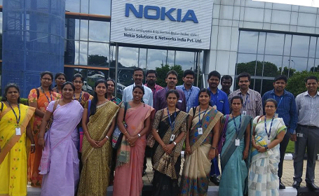
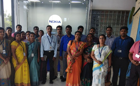
Nineteen faculty members from various disciplines of KCG College of Technology, Karapakkam, Chennai visited Nokia Solutions & Network Systems, Oragadam, on 18th September 2017.
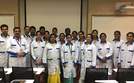
All left the institution by 9.15 am and reached the factory by 10.30 a.m. All were welcomed by Mr. G Agni, Team Leader, Filter Production, and he gave a brief idea on what is happening at the factory. He also explained the activities that are carried out for the students, through university/institute collaboration, internships, summer camp, hackethon, etc., Then Mr. Ramachandra Rao, Faculty Trainer, discussed the safety and precautions to be taken inside the factory, while visiting the shop floor. All the participants were given a static voltage protection garment to wear, to safe guard the components/devices that are manufactured. Then Mr. P Karthikeyan, Manager – Industrial Engineering and Automation, discussed the business/products that is happening/developed in the factory, through a video presentation. To clarify everyone’s doubts Nokia is still developing cell phones which are marketed through HMD Global. The other products developed and manufactured by Nokia are Base station controllers, Base station transceivers, etc. Globally Nokia without mobile manufacturing has nearly 1 lakh employees. Most of the design and developments were carried out at Nokia Bell Labs at Shanghai, which is China’s biggest city and the global financial hub. Nokia is currently doing its research on 5G technology in mobile communication. Its quality for customers is based on I Own Quality. He explained about the various processes going on in the Oragadam factory, which is 8 years old now.
The participants were then taken to visit the shop floor where the production and warehouse is made. The stock are been carried through Automated Guided Vehicles (AGVs). The staff at Nokia should be SMT certified only then they’ll be allowed to entry into the shop floor for working. They are also given Kaizen awards for their performance. They also have 5 S team awards for housekeeping. KPI charts are displayed for indicating the performance indications.
Different sections such as assembling, moulding, packaging, picking & placing, etc. were shown. Initially the designed PCB weighing nearly 250 grams were inserted into a stencil printing machine to scoop the solder over the PCB uniformly. In this machine the solder will be in the semi-liquid stage. Then the PCB is given to a solder thickness measuring machine, which measures the thickness over the PCB, which is also manually checked for any empty pads. Now the components are inserted using the SMT Component Populating machine, which can populate 75,000 components per hour. The SMT components are placed in feeders which are automatically fed into the populating machine for component insertion. The population is automatically made by the programs that are fed based on the PCB. Next the populated PCB are inserted into a PCB counting machine to count the populated PCB, where the components are semi-soldered. Now pre-soldering inspection is made manually to verify all the components are inserted or not. Then the PCB is inserted into a Reflow Oven, which is approximately 10 meters long, where the temperature is raised to nearly 250 degree for doing the soldering. Then the PCB is send to a blower for cooling. After the PCB comes to the normal room temperature, the PCB is arranged in the PCB stack. Then the PCB is given for testing one by one to check the soldering manually, and then by inserting into to Automatic Optical Inspection (AOI) machine. Then the tested PCBs are given to a PCB depaneling machine, to remove the unwanted PCB. Then by using in-circuit tester the unwanted solders are removed. Then the unit is tested for modular function test, where each and every modules in the PCB is tested separately. The failure rate at this stage is less than 0.6 %. Next is the unit level assembling for filters and RF sections. Most of the filters and resonators are fixed manually. Then tuning is made for the required frequency. Agilent test machines are used for this purpose. Again fine tuning is made at the second stage of tuning. Finally RF assembling and heat sinks are fixed. Screws are fixed both manually and using robots. The completed device is given for Ingress Protection testing. The final device weights about 50 Kg. The tested unit is send for packing, where the required accessories and manuals are kept along with the device. The packed unit is placed in the warehouse for delivery based on client’s requirement.
Then we visited the warehouse section we were able to witness both manual working and automated working in this section. Automatic Guided Vehicle with object detector is used to carry the components and materials from the warehouse to the manufacturing unit. The stack section was huge. Based on the material, they classify the bay into three. Bay A has materials with very expensive, bay B with medium expensive and bay C with less expensive such as screws, washer, etc.,
Then visited the training section, where AKS (awareness, knowledge, skill) model is adopted to train the new joining staffs. They also demonstrated the signal transmission in GSM architecture with a model. The Oragadam factory manufactures the BTS part in the GSM architecture.
The factory visit comes to an end by 1.30 p.m.
After the lunch Mr. Ramkrishna Patra, Head – Manufacturing Solutions & IoT Cluster joined with us along with Mr. G Agni and Mr. P Karthikeyan for a detailed discussion. Faculty members interacted with the officials of Nokia about establishing relationship between KCG College of Technology and Nokia in view of R&D, student projects, internships and product developments. They have happily agreed to extend their hands to associate with us for the benefit of the student community. Finally, we left the factory by 4:30 pm after the fruitful discussion.
We extend our sincere thanks to the Management and Principal for providing us the opportunity to get an industry exposure by arranging this factory visit. Also we extend our heartfelt thanks to the officials of Nokia for permitting us to visit their factory operations and for their acceptance for further collaborations.
Following are the faculty members participated in the visit.
- R Dhanalakshmi, Professor, CSE
- Poonkavithai, Professor, CSE
- R Anandh, Associate Professor, IT
- Jose Anand, Associate Professor, ECE
- S Cloudin, Associate Professor, CSE
- Sreekantha Kumar V P, Associate Professor, IT
- N Sivakama Sundari, Associate Professor, EIE
- V Hema, Assistant Professor, CSE
- S Soumya, Assistant Professor, CSE
- Minu Thomas, Assistant Professor, CSE
- A Anju, Assistant Professor, IT
- Krithikaa Venkat, Assistant Professor, IT
- Presanna Prabhu, Assistant Professor, Mechanical
- A Arvin Tony, Assistant Professor, EEE
- N Loganathan, Assistant Professor, EEE
- Aida Jones, Assistant Professor, ECE
- Feba Sosa Abraham, Assistant Professor, ECE
- M. Lavanya, Assistant Professor, EIE
- M Ramya, Teaching Assistant, EEE